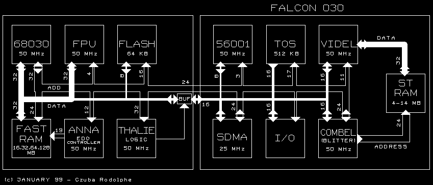
CT2 ARCHITECTURE
(c) January 99, Rodolphe Czuba
1/ PRESENTATION
As you can see on the picture lower, the hardware architecture of the CT2 is built with two 32-Bit buses, adverse the Falcon built with a 16-Bit DATA bus (except the 32-Bit DATA bus between ST-Ram and VIDEL).
The FAST-Ram of the CT2 considerably increases the performances of the Falcon which have only a 16-Bit singe memory (ST-Ram) used by both the CPU and the VIDEO/SOUND chips.
You can now run the programs in True Color mode as quick as in 16 colors mode because the programs executions are not decreased by the big video modes accesses!
More, the BURST mode of the 68030 is now used to read and cache 4 LONGWORDS with only 12 CPU (50MHz) cycles !
The WRITE accesses have been improved from 6 (REV A) to 4 cycles at 50 MHz !
In fact, the Falcon becomes a simple 16-Bit Super I/O card managed by the CENTurbo II...
So, the ST-Ram becomes the VIDEO/SOUND ram; what it is called 'CHIP-Ram' in the AMIGA world: the ram uses by the chips (BLITTER, VIDEO, SOUND).
The FAST-Ram becomes the MAIN ram which must be used as much as possible by the CPU. This architecture is near the one of the PC...
The heart of the CT2 is done with 2 chipsets named ANNA & THALIE which manage the following features:
ANNA:
- 60ns EDO DRAM 50 MHz Controller performing BURST READING with 5,2,2,2 clock cycles at 50 MHz (real 32.5 MB/s) and WRITING with 4 clock cycles at 50 MHz (real 38 MB/s !). See the benchs...
- Hardware Watchdog of 6 us.
- Generation of the 500 kHz clock for the two ACIA.
THALIE:
- FPU communication.
- Logical interface to access the Falcon 68000 bus at 50 MHz.
- DATA buffers.
- Accesses to the FLASH at 50 MHz.
- Accesses to the DSP at 50 MHz.
- Accesses to the ACIAs at 50 MHz.
- Accesses to/from the SDMA in SLAVE/MASTER mode.
- INTerrupt level 4 and 2 (VBL and HBL).
- Clocks (except for the ACIAs).
- CT2 setting registers.
2/ NEW METHODSMany software developers have to change their programming methods of the Falcon because, in many cases, the use of the FAST-Ram by the CPU is very more advantageous than the use of any others techniques designed to avoid the slowness of the ST-Ram.
This is a fact for those who have used the DSP to compute things that can now be computed faster by the CPU in FAST-Ram. Programmers have now to use the DSP only for the things for what it was originally designed (matrix, FFT, and so...), and don't forget that the time to transfer to and from the DSP (by a 8-Bit bus !) is became important opposite to the time about the FAST-Ram.Furthermore, an important effort must be done to code LONGWORDs and align the code (C programmers: code with ASM !) at least on 32-Bit boundaries, or better, on 16 bytes boundaries (4 LONGWORDs = 1 cache LINE).
This is necessary if you want to use the CACHE BURST at the better performances.
Meanwhile, you have to know that the 'WRAP AROUND' of the 030 is set OFF by the CT2 to avoid a performances decrease with the majority of the softwares which don't respect the alignments on 32-Bit boundaries.
The VL-BURST (Variable Length) allows the CPU to fill only the end of the cache line without filling the begining of this line.
By example, if you run code at $01025480, the CPU bursts an entierely line of the cache from the addresses $01025480, $01025484, $01025488 and $0102548C.
If the CPU begins to burst from $01025488, it will stop after reading the second LONGWORD at $0102548C and will not go to read the two first LONGWORDs at $01025480 and $01025484 ! What it would have done with the WRAP AROUND...
In the most cases, 4 CPU cycles (2+2) are economised because it is rare the CPU needs these two first LONGWORDs, except with some not very used addressing modes...For more informations about the caches of the 68030, please refer to the '68030 USER'S MANUAL' (chapters 6 & 7) from MOTOROLA.
