Atari Falcon custom chips decap initiative
Beware, this “Donate” button charges 3% of the sum you donate, so if you are about to wire a bigger amount, better use Paypal Family&Friends directly at mirokropacek
Also beware, if your native Paypal currency is e.g. US Dollar and Paypal encourages you to sent the payment as EUR, it will convert your payment with a terrible rate. Always pay in USD (there should be an UI option for that, I have already received several USD payments as you can see bellow).
Or you can use Wise
Or if you prefer EU IBAN transfer: SK37 5600 0000 0061 8230 8002
(let me know in the message for recipient which name/nickname should I use for publishing your contribution)
(if nothing from the list above works for you and you desperately want to contribute, please contact me at miro.kropacek at my gmail account and we figure something out … Wise let me have a national account for many countries for example)
Final sum for decap: $8,021 USD.
| Contibutor | Contribution |
|---|---|
| (anonymous) | 100 USD |
| Lukasz Jokiel | 20 EUR |
| evldhs | 50 USD |
| Andrej Gerbec | 100 EUR |
| Thibault Bernard | 70 EUR |
| Przemyslaw Szeremiota | 25 USD |
| Matthias Arndt | 200 EUR |
| Martin Faxér | 100 EUR |
| Simon Yardley | 28.10 EUR |
| Stefan Lindberg | 53.49 EUR |
| Stephane Capo | 15 EUR |
| Olivier Jan | 54.75 EUR |
| Kevin Hulse | 100 USD |
| Douglas Little | 250 EUR |
| Bartłomiej Sroczyński | 50 USD |
| Anders Granlund | 100 EUR |
| Chris Holland | 56.19 EUR |
| Sedma | 50 EUR |
| Janez Valant Jerman | 100 EUR |
| Sporniket | 15 EUR |
| Miroslav Nohaj | 25 EUR |
| tzeb | 50 EUR |
| atari.sk | 200 EUR |
| Cosmos Atari | 50 EUR |
| Wietze Spijkerman | 50 EUR |
| Roman Lukovics | 100 EUR |
| Cyprian Konador | 25 EUR |
| kohli79 | 50 EUR |
| Stuart Duncan | 117.32 USD |
| Joaquin Ferrero | 100 EUR |
| Ronald Hall | 24.52 EUR |
| tOri | 22.51 EUR |
| Erez Yaary | 150 EUR |
| Joseph Ceklosky | 22.58 EUR |
| David Galvez Carles | 40 EUR |
| nerve | 50 EUR |
| Fredrik Olsson | 100 USD |
| Peter Slegg | 20.01 EUR |
| SidecarTridge | 150 EUR |
| Daniel Hedberg | 50 USD |
| foft | 213.21 EUR |
| Thomas Heimann | 100 USD |
| Philsan | 50 EUR |
| Francois Galea | 68.03 EUR |
| insane/tscc | 150 EUR |
| tOri | 25 EUR |
| Mickael Pontier | 50 USD |
| Nokturnal | 150 EUR |
| jym | 30 EUR |
| Trixster | 10 EUR |
| Atarian Computing | 100 EUR |
| Adam Kłobukowski | 100 USD |
| Mathieu Demange (sigmate) | 600 EUR |
| Steffen Thomas | 150 EUR |
| Laurent Sallafranque | 90 USD |
| Simon Abejansky | 50 EUR |
| Jesse Burns | 100 USD |
| Sascha Springer | 100 USD |
| Markus Fichtenbauer | 100 EUR |
| Devander | 100 EUR |
| Questor | 100 EUR |
| Patrick - MEX68KECB | 50 USD |
| tOri | 25 EUR |
| Denis Karimani | 150 USD |
| Martin Faxér | 100 EUR |
| Badwolf | 60 EUR |
| Geir Øyvind Vælidalo | 50 USD |
| tOri | 40 EUR |
| John Sohn | 50 USD |
Funds collected (conversion rate 1 EUR = 1.17 USD): $6,654.49 USD.
What is this about?
As you are certainly aware, nearly each computer from the golden era of home computers (1970s - 1990s) was designed to use one or more custom integrated circuits. Custom means that it wasn’t a component you could purchase in any store (so called commercially available off-the-shelf = COTS) but it was designed usually in-house and then ordered to be manufactured as a private contract.
The Amiga is famous for having many great custom ICs but as mentioned, basically any home computer from that era had some, the Atari Falcon030 not being an exception. Falcon’s custom ICs are an evolution of the chipset found in the Atari STE: GST MCU (GLUE + MMU + BLiTTER) became the Combel (Combo) chip, the Shifter became the Videl and the DMA became the SDMA.
Over the time, various interesting resources and projects have seen the light of day:
-
FX68K 68000 cycle accurate SystemVerilog core by ijor (Jorge Cwik)
-
FX ST Blitter by ijor (Jorge Cwik)
-
Atari ST Shifter decap by ijor (Jorge Cwik) (on AF you can find posts about further decaps / analysis of the MCU and MMU, too)
-
Blitter re-creation initiative by Exxosforum folks
-
Atari ST ASIC designs by Christian Zietz (see also Atari STE GST MCU + GST Shifter Simulation based on them!)
… and some more (unfortunately, there is quite a chaos when it comes to finding the actual drawings and sources). Using those but also with a lot of patience and trial and error, people started building their own cores for the MiST(er) or even from scratch like the zeST or Suska.
With some simplification one could say that building your own cycle-accurate ST and maybe even STE machine in FPGA is a real possibility today (and not only in FPGA, see the H5 Phoenix or Atari ST ATX). However, when it comes to Falcon, this is a whole different matter. While the physical replica of Falcon PCB has been attempted at least three times:
-
F030NG by Centuriontech (Pavel Salac, cancelled)
-
Falcon motherboard recreation by Cosmos (ongoing), followed by RE Falcon 030 by Suavek (ongoing)
-
Falcon Re-Imagined by Wizztronics (see also the AF thread, older website and their Facebook page, ongoing)
the actual chips must have been supplied either from a real Falcon or purchased from BEST Electronics or Wizztronics (from their limited supply of new old stock, of course). Apart from that, there was only one attempt to actually produce an enhanced replica of the Videl chip - the SuperVidel project and even that one was based on guesswork, Hatari source code and the partial documentation available from demo coders.
So it’s time to change that!
But why, really?
There are basically two, okay, three main bullet points for me:
-
to be able to switch your broken Videl (Combel, SDMA) chip for a new one, in case it gets damaged (Videl is the most common offender here, often due to usage of the original, non-recapped, power supplies)
-
to encourage development of new Falcon PCB replicas. Why? Well, let’s say that the original Falcon PCB has so many defects and cheap solutions that it’s miracle it is even working. And of course it open gates to further expansion, like onboard SATA/USB/Ethernet, better CPU/DSP etc
-
and the last but not least: to be able to uncover the custom ICs’ secrets! There’s a couple of clues (both from leaked TOS 4.04 source code and internal documents about the Dallas Falcon project) that Atari had in the works a true chunky-oriented 8bpp video so who knows, maybe there will be some clues about that.
Humble beginnings
Of course, I had this idea in my head for a long time. Back in January 2018 I contacted ijor about his decap work for 8-bit and 16-bit Atari machines and inconspicuously asked about any hope that he’d do the same for the Falcon. He replied that it’s not on his radar but gave me some insight about taking pictures of the die:
Well, it would be hard, of course, and would take a lot of time. But it is certainly feasible. Can’t be very precise without knowing the scale of the size of the Falcon chips.
[…]
You have to either convince somebody to take the pics for free, or pay a specialized lab, which would require collecting some money. Not easy to get somebody to do it for free, especially on not so old dies because it would take lots and lots of pics.
Fast forward to October 2024, I suddenly remembered about our chat when reading a thread on Exxosforum. As you can see, I got more or less the same reply. However this time I decided to follow through and actually investigate what it would really take. So I contacted ijor once again.
Basically, ijor advised me the following:
-
be prepared that the project will take many months, probably years but it has to be started at some point
-
get a chipset to decap (ideally working, considering the enormous effort involved)
-
collect money for at least one chip (with his estimate being about $1,000 USD per chip … please note this was before he actually saw the lowpres die shots)
-
send him one sample to forward to the lab for decap and producing high rez images of the die
-
once the lab performs the work, he will post the images in a public place
-
eventually, ijor, or somebody else, (or AI), or some kind of joined effort would produce reverse engineered schematics
He reminded me again that this might take years and that he cannot commit himself at all or to make any kind of promises whatsoever but when it comes to it, his work would be for free. All the money would be spent on the process of acquiring the die pictures.
So that got me thinking. BEST sells those ICs for $45 per piece, so perhaps this is a good opportunity to purchase them before they run out of stock. So that would solve the chipset availability problem (no need to desolder them from a Falcon). Then there’s the reliable (and somewhat cheap-ish) lab in Taiwan which has experinece with similar jobs. And most importantly, I’m in the mood to really do it! And so I did. I purchased all three ICs (Videl, Combel, SDMA) from BEST and shipped the Videl (for starters…) to the lab.
And in March 2025 we got …
… a low rez sample of Videl’s die!
So here we are
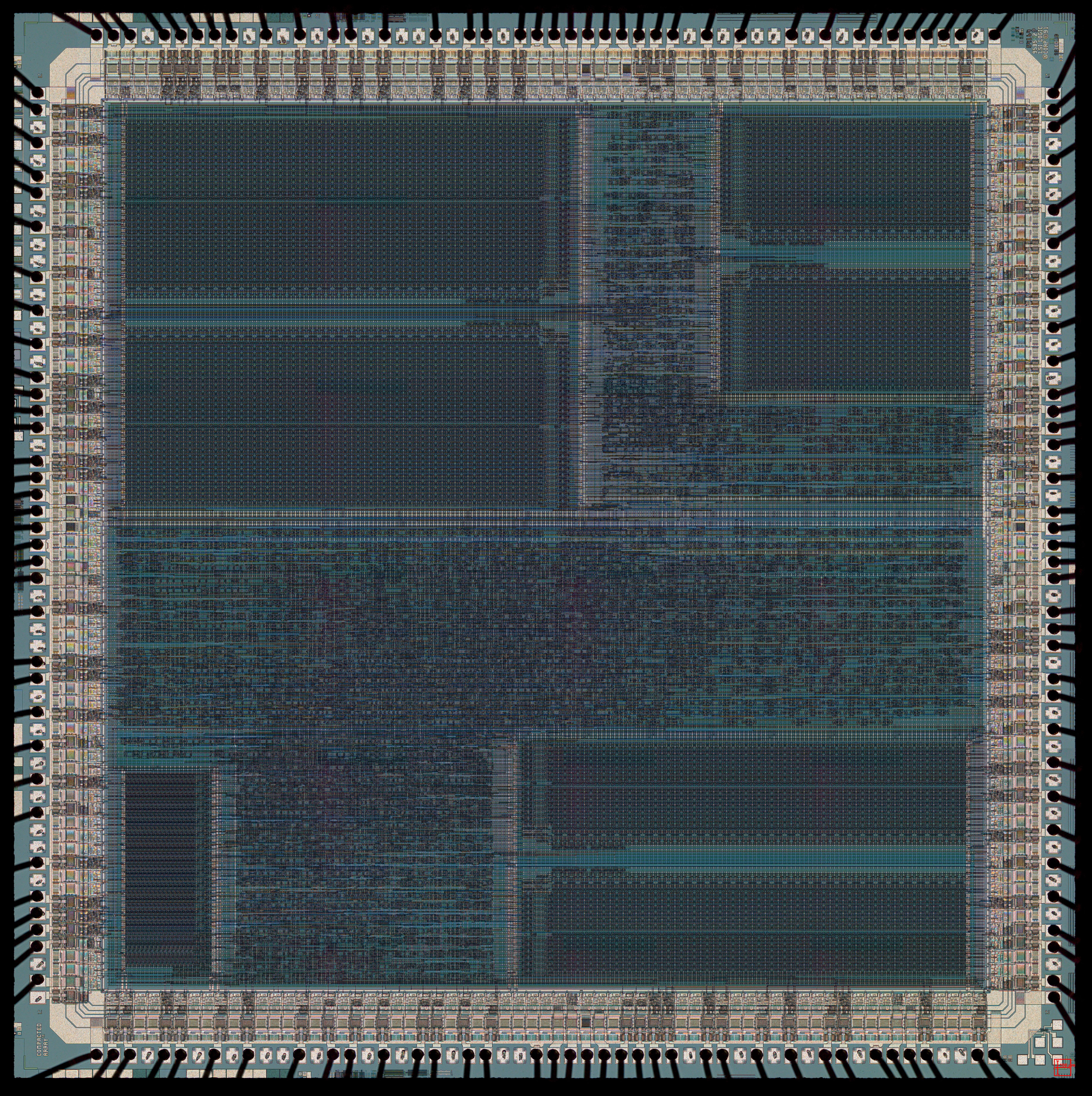
With the die’s image several things became clearer. The most important one being that the die is pretty big. In comparison, this die is about 2.5 times larger than the one on the ST chipset. And it also uses a more modern, and hence, smaller, CMOS process. This would mean that the lab cost will be much higher. The lab charges by picture. Bigger die require more pictures. And also the more advanced CMOS process will require using higher resolution pictures, which again, means more pictures.
Our initial estimate was something between $2,000 USD and $3,000 USD and unfortunately, this has proven to be a very optimistic one. The final price for the work is $8,021 USD and there’s nothing we can do about it, it must be paid. :-(
The reason for the higher quote is a combination of factors. In the first place we underestimated the total number of raw images required considered the die size and the higher microscope magnification required. Videl required more than 7,500 high rez pictures not only due to the die size but also because it required a much higher magnification level – usually 200x is more than enough for ST chips but in this case it required 500x. Therefore most dies used in old school systems take less than 1,000 pictures, some even less than 500 pictures (and would therefore cost way below $1,000 USD to decap).
For explanation, the die is built with multiple layers one on top of the other. Metal layers are usually at the top and being wide and bright you can’t see much of the actual silicon layers below.
The decap process is to take an image for one layer and then remove it with a process called, well, delayer. Once that layer is removed, they take an image of the lower layer that is now fully visible. This repeats until all the relevant layers were processed. Sometimes you don’t need to remove all the layers. But in most cases you need at least to remove the metal layers. Even then, it won’t be easy to read the logic. It will probably take quite some time.
Now that we recieved the images we can start the long and tedious process to convert this to netlist, schematics, and/or HDL (Verilog/HDL). The exact step could vary depending on the case.
Donations
There are two aspects to it. The first one being, of course, that $8,021 USD is quite a lot of money. So that begs the question whether other people wouldn’t be willing to contribute to a good cause. The second aspect being that I couldn’t give ijor the go-ahead unless I was sure I got the funds ready which could take months if I relied only on public funding, after which many things may have changed (like the price, or the lab’s availability etc). So I decided the following:
-
I will be the one paying the bill, no matter what. Not gonna lie, I was expecting something like $3,000 tops and now I have to pay more than twice as much but that’s the risk I was willing to take, so no regrets here.
-
As soon as I pay the bill, I’ll offer the die shots to anyone willing to work on them, with the goal of publishing his or her work immediatelly, i.e. I would postpone the release for some time to give this open source developer a head start before anyone else (especially entities which would like to use the die shots for their own, closed source, products).
-
In a few months’ time I will release all the die shots for everyone, making them available for both commercial (e.g. for the Apollo) and open source developers without further restrictions.
-
For a better idea what to expect, I’ll remind you of another campaign, the restoration of Geneva/Neodesk archive. For those unaware, in October 2016 Antoni Sawicki, also known as tenox (see also his Atari System V website!), contacted Dan Wilga with an inquiry about restoration of his old Atari TT hard drive. In May 2017 Dan’s hard drive content had been recovered for a hefty $1,900 USD. In addition to that, Atarian Computing (Joshua Kaijankoski) created a petition to show Dan how much anticipated the release of his products was. However it took nearly one more year to actually get the (now freeware) updated executable files and then another six years the source code!
-
So you see, your donation wont turn into a FPGA Falcon overnight but with some luck (and patience), we might see something interesting over the course of a few years… not to mention the motivation boost for everyone invoved to actually start reverse engineering all three chips.
Timeline
12.02.2026
The lab provided the final invoice – $2,795 USD. Phew. ;) In the meantime, ijor couldn’t resist and started working on Combel, too.
But it is going slowly. It turns out that Combel is much more difficult than Videl. This is for a couple of reasons. One is the intrinsic characteristic of the die. But also it turns out the Dmitry’s pics are not as good as we had hoped. To be more precise, the pictures themselves are great. The problem is the condition of the die. The die seems to be damaged in multiple spots. Not exactly sure why. May be it is because the decapsulation method he uses.
The current situation is following: the lab processed a Combel chip (so we basically have two of them decap’ed now – Dmitry’s and this one). But we didn’t ask for high rez pictures for all the layers, as we did with Videl. Otherwise it was going to cost us about the same that we paid for Videl. So, we don’t have lab high rez for Combel top layer. We did ask them to take lowish/med rez pictures of the top die, though. That was done mostly to be sure that both Combel chips are exactly the same revision. Just in case there are multiple ones.
In some cases those lower rez pictures can help to decode the damaged die spots, but not in all of them. It is not the end of the world, though. They aren’t too many spots. And it is usually possible to figure out the layout anyway. It just makes the process slower.
Anyway, some surprising discoveries on the way!
07.12.2025
For Videl, a couple of verification steps were needed. ijor completed the first a few weeks ago. Still trying to find the time to perform the last step – we are very close to be able to release a netlist shortly!
On the Combel front, the decision to remove metal layers only turned out to be more problematic. The lab usually doesn’t send a half-done work to the customer plus we need some other things which Dmitry couldn’t provide (like X-Ray images) so we have decided to order a full decap work for Combel, too. Of course, it wont cost as much as the Videl one, expectations is about $2,700 USD.
14.11.2025
Combel has arrived at the Taiwanese lab for metal layer removal. After this is done, it should be easier for Dmitry to prepare cleaner die shots.
07.10.2025
It may look like there’s nothing going on but ijor has been busy with tracing the Videl die. After just a few months he was able to perform the first simulation waveform produced from a netlist extracted from the die shot.
Also, we are quietly working towards better die shots for the Combel and SDMA but it takes time.
31.07.2025
Dmitry sent us first images of delayered SDMA.
22.07.2025
Dmitry sent us the complete set of Combel die shots with the metal layer removed.
15.07.2025
Dmitry sent us first images of delayered Combel. The quality is excellent, we’re still refining the process with him to get the best Combel & SDMA images possible.
08.07.2025
Today I wired the whole $8,021 USD from my bank account to Taiwan. Thanks to all of you who have contributed I didn’t go bankrupt. :-) We are still not finished though, there’s ongoing work on Combel and SDMA.
30.06.2025
ijor has started a technical thread about this effort on AF: https://www.atari-forum.com/viewtopic.php?t=45152.
23.06.2025
Received invoice from the lab. They even charge a 6% credit card handling fee. Perhaps we’ll try to wire the money directly to their bank via Wise or so.
11.06.2025
Received the final quote from the lab: $8,021 USD !
07.06.2025
ijor managed to stitch Dmitry’s images the same way as he did with the ones from the lab.
31.05.2025
Received Dmitry’s work on Combel and SDMA. Images are a bit worse compared to Videl but but this might just be related to the die characteristics and the different fab process. Still excellent images.
23.05.2025
ijor managed to process all images with his scripts: full resolution images were split in four quarters. Total resolution is approximately 67,500 x 67,500 pixels. A single combined image would exceed the JPG maximum resolution and would require a PNG, or BigTIFF, file taking several gigabytes. Then there are single die image scaled down 3% just to stay below the 64K JPG maximum pixel resolution. There is no significant difference with the full resolution images.
21.05.2025
Received last batch from the lab - substrate and poly layer images.
The good news is that about half the die is just RAM. All the RAM cells are identical, there is no need to reverse engineering each RAM cell. There is some work to be done at the RAM decoding and read write logic. But that should represent much less work in comparison. It is almost like half the work is already done.
14.05.2025
Received Dmitry’s work on Videl. He isn’t able to delayer the chip but nevertheless the quality of the images is superb. To our shock, while the lab is taking their time with just the one chip, Dmitry was able to offer complete decapping of all three chips in a very near future, amazing!
03.05.2025
We’ve got all pictures of the top and bottom layers directly produced by the microscope camera.
28.04.2025
Got in touch with Dmitry, an extremely talented fellow who was able to decap many ICs in the past. We discussed our options with him, in the end thanks to another great fellow, Mathieu, we could send him another batch of the Videl / SDMA / Combel triplet (the first one went to ijor / the lab) to get his hands dirty.
22.04.2025
High rez picture of the bottom metal layer received as well as a new take of the top metal layer one.
01.04.2025
High rez picture of the top metal layer received. It is not really possible to read the logic yet. But there is something interesting. There are four regular areas located at the four corners. These most likely are RAM, or conceivable, one might be ROM.
26.03.2025
Low rez sample of Videl’s die received. This image is at low resolution and it’s just for the purpose of getting an idea of the die characteristics.
Future
We ended up with much more than what we had anticipated in the beginning:
-
fully delayered Videl chip by the professional Taiwanese lab (ok, we did anticipate this one ;))
-
decaped (but not delayered) Videl chip by Dmitry
-
decaped (but not delayered) Combel and SDMA chips by Dmitry
When Dmitry took up the challenge, we were curious about the actual difference in quality of the supplied results. And that was a really good call because we have found out that the lab is able to do complete delayering while Dmitry can provide excellent images but only with all layers together. In the end, it doesn’t seem to be a showstopper but still, it will make reverse engineering much more pleasant with each layer separated. We are still in talks with Dmitry about his options for the Combel and SDMA.
Furthermore, the most important outcome is that we are now more or less sure that we wont need to pay the Taiwanese lab any more money. This comes from the fact that we could compare professional die shots with his and decide what needs to be improved / focused on. Without this comparison we couldn’t reliable decide whether we need to order the Combel and SDMA from the Taiwanese lab or not. Of course, feeling that decaping the other two chips at the lab could cost as much as the Videl certainly encourages us to focus on Dmitry’s images ;-) but still, it’s good to know that the decision is based on facts.