|
|
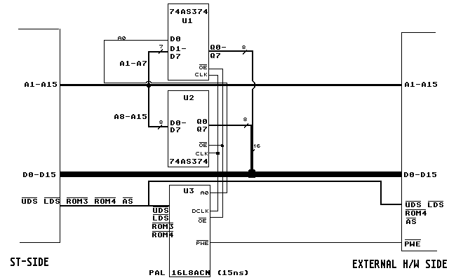
15.6.5 Cardridge Port Interface
Cartridge Port Interface
Abstract
The Atari ST's 128 Kbyte read-only cartridge port can be
transformed into a 64 Kbyte read/write port by using this circuit.
Writing to this port is slower than reading it by a factor of two,
approximately. It can be written to at a speed of 76 Kilowords per
second.
This interface can be built by using only three chips, two AS-TTLs
and a PAL - a total parts cost of less than $15.
How It works
1. Background Information
The ST brings out 15 address lines (A1-A15), 16 data lines
(d0-D15) /LDS, [*] /UDS, /AS, /ROM4 and /ROM3.
Of these signals, /UDS, /LDS, and /AS have the same meaning as
they do for a 68000 CPU. A1-A15 are the least significant 15 address
lines. D0-D15 are connected internally to the ST's data-bus. /ROM3 and
/ROM4 are generated by the MMU, and are output signals, which tell the
external hardware which of the two banks is being addressed. /ROM4 is
activated when the 68000 tries to read address 0xfa0000-0xfaffff.
/ROM3 is activated when the 68000 tries to read address
0xfb0000-0xfbffff (note that the names of these signals are
counterintuitive; ie. they have been correctly written above).
Any and all hardware connected to this modified port must be fast
- fast enough to run with no wait-states and fast enough to tolerate
the decoding delays introduced by this circuit. I've used 200ns static
RAM chips without any trouble.
It is advisable to use /ROM4 to time any external hardware you
build (in preference to /AS), since /ROM4 contains the necessary delay
to ensure the addresses are stable when it is activated. (At least
this is what I assumed, and it worked.)
The data for write operations is produced by the two AS-TTL
latches[*] used in the circuit (see below.)
3. Operating Principle
Construction
The schematic should help in this department. Constructing this
gadget is easy and cheap. The hardest part might be trying to find a
connector for this port. You can get one from:
Douglas Electronics,
1-415-483-8770
(part number 33-DE-40. $10.00 per piece)
[*] Another problem you might face is getting the PAL programmed.
If you don't know of a way to get the PAL programmed, you could use
discrete logic chips to build the state machine.
4. Building it
The pin-outs given in the User's guide are CORRECT. The pin-outs
given in the "Internals" book are WRONG. Follow the
schematic. You can get the pinouts for the '374s from an ASTTL or FAST
databook. The PAL16L8's pinouts are given below.
[*] You guessed it - I'm not connected with D.E. although I and a
number of others have purchased these connectors from them.
PAL Pinouts in the external "Program" Folder
A preceding slash implies an active-low signal.
Note that the line called "help" is shown as
"NC" since it is to be left unconnected.
Anees Munshi.
Copyright © Robert Schaffner (doit@doitarchive.de) Letzte Aktualisierung am 23. Mai 2004 |
|
|